| CPC H01L 29/41733 (2013.01) [H01L 21/76224 (2013.01); H01L 27/088 (2013.01); H01L 29/66742 (2013.01)] | 20 Claims |
|
18. A device, comprising:
a substrate;
a first transistor on the substrate, the first transistor including a plurality of first semiconductor nanostructures corresponding to a channel region of the first transistor;
a second transistor on the substrate, the second transistor including a plurality of second semiconductor nanostructures corresponding to a channel region of the second transistor;
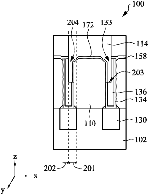
a source/drain region in contact with the plurality of first semiconductor nanostructures and the plurality of second semiconductor nanostructures along a first direction;
a first dielectric fin structure and a second dielectric fin structure adjacent to opposite sides of the source/drain region along a second direction that is transverse to the first direction, each of the first and second dielectric fin structures including a respective upper surface, a lower surface, and an intermediate surface that is disposed between the upper and lower surfaces; and
a silicide layer on a top surface and side surfaces of the source/drain region, the silicide layer disposed on the intermediate surfaces of each of the first and second dielectric fin structures.
|