| CPC H01L 29/41733 (2013.01) [H01L 21/0259 (2013.01); H01L 21/28518 (2013.01); H01L 21/823412 (2013.01); H01L 21/823425 (2013.01); H01L 21/823475 (2013.01); H01L 21/823481 (2013.01); H01L 24/08 (2013.01); H01L 24/80 (2013.01); H01L 25/0657 (2013.01); H01L 25/18 (2013.01); H01L 25/50 (2013.01); H01L 27/088 (2013.01); H01L 29/0665 (2013.01); H01L 29/401 (2013.01); H01L 29/42392 (2013.01); H01L 29/78696 (2013.01); H01L 2224/08145 (2013.01); H01L 2224/80895 (2013.01); H01L 2224/80896 (2013.01); H01L 2924/1431 (2013.01); H01L 2924/1434 (2013.01)] | 20 Claims |
|
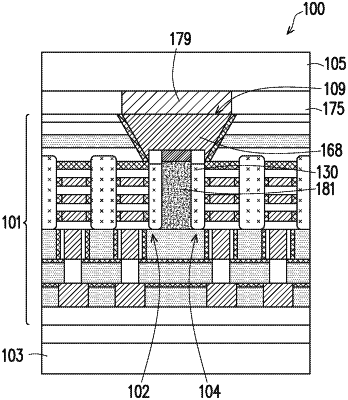
1. An integrated circuit, comprising:
a first chip including:
a substrate including:
a first semiconductor layer;
an etch-stop layer on the first semiconductor layer; and
a second semiconductor layer on the etch-stop layer
a first gate all around transistor on the substrate and having a source region; and
a backside conductive via extending through the substrate to the source region, wherein the conductive via extends through the first semiconductor layer, the etch-stop layer, and the second semiconductor layer.
|