| CPC H01L 29/401 (2013.01) [H01L 21/0337 (2013.01); H01L 21/28518 (2013.01); H01L 21/31155 (2013.01); H01L 29/456 (2013.01)] | 20 Claims |
|
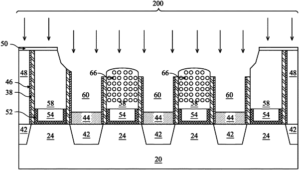
1. A semiconductor device comprising:
a gate disposed over a substrate;
a source/drain region adjacent to the gate, wherein the source/drain region is covered by a silicide layer;
a first hard mask covering the gate, wherein the first hard mask comprises amorphous silicon and nitrogen; and
a second hard mask covering the first hard mask.
|
|
9. A semiconductor device comprising:
a first fin extending from a semiconductor substrate;
a first gate stack on the first fin;
gate spacers on the first fin, the gate spacers covering opposite sidewalls of the first gate stack, the gate spacers extending above the first gate stack; and
a first hard mask on the first gate stack, the first hard mask being between the gate spacers, the first hard mask comprising amorphous silicon.
|
|
17. A semiconductor device comprising:
a mask over a gate electrode, the gate electrode being over a substrate, wherein the mask comprises amorphous silicon with N—Si bonding;
a gate contact coupled to the gate electrode, the gate contact extending through the mask;
a source/drain region on the substrate, the source/drain region neighboring the gate electrode; and
a silicide layer on the source/drain region, wherein the silicide layer comprises titanium.
|