| CPC H01L 29/0665 (2013.01) [H01L 29/0649 (2013.01); H01L 29/42392 (2013.01); H01L 29/66742 (2013.01); H01L 29/78696 (2013.01)] | 20 Claims |

|
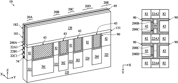
1. A device comprising:
a substrate;
a first stack of semiconductor nanostructures vertically overlying the substrate;
a gate structure surrounding the first stack of semiconductor nanostructures and abutting an upper side and first and second lateral sides of the first stack, the first and second lateral sides being opposite each other;
a first epitaxial region laterally abutting a third lateral side of the first stack;
a second epitaxial region laterally abutting a fourth lateral side of the first stack, the fourth lateral side being opposite the third lateral side, and the second epitaxial region spaced apart from the first epitaxial region in a first direction;
a first inactive fin laterally abutting the first epitaxial region in a second direction transverse to the first direction; and
a second inactive fin laterally abutting the second epitaxial region in the second direction transverse to the first direction, and each of the first and second inactive fins laterally abuts the gate structure on opposite sides of the gate structure such that the second inactive fin is physically separated from the first inactive fin by the gate structure.
|