| CPC H01L 27/156 (2013.01) [G09G 3/32 (2013.01); H01L 33/005 (2013.01); G09G 2300/0426 (2013.01); H01L 25/167 (2013.01)] | 13 Claims |
|
1. A display module comprising:
a first substrate;
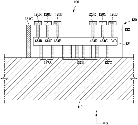
a plurality of micro-pixel controllers provided on an upper surface of the first substrate and comprising a second substrate;
a plurality of pixels comprising a plurality of inorganic light emitting diodes (LEDs) provided on an upper surface of the second substrate; and
a driver integrated chip (IC) configured to transmit a driving signal to the plurality of micro-pixel controllers,
wherein each pixel of the plurality of pixels comprises at least two inorganic LEDs among the plurality of inorganic LEDs, and
wherein each micro-pixel controller of the plurality of micro-pixel controllers is electrically connected to inorganic LEDs of at least two pixels among the plurality of pixels,
wherein each micro-pixel controller of the plurality of micro-pixel controllers comprises:
an upper connection pad provided on the upper surface of the second substrate and electrically connected to an inorganic LED of the inorganic LEDs,
a pixel circuit provided in the second substrate and electrically connected to the upper connection pad through a first blind via extending from the pixel circuit to the upper surface of the second substrate in a vertically upward direction, and
a plurality of lower connection pads provided on a lower surface of the second substrate and electrically connected to the pixel circuit through a plurality of second blind vias, respectively, and
wherein each of the plurality of second blind vias extends from the pixel circuit to the lower surface of the second substrate in a vertically downward direction opposite to the vertically upward direction and is electrically connected to an upper wiring pad of the first substrate,
wherein the upper connection pad comprises a cathode pad electrically connected to a cathode of the inorganic LED, and
the cathode pad is electrically connected to a lower connection pad provided on the lower surface of the second substrate through a via hole extending from the upper surface of the second substrate to the lower surface of the second substrate in the vertically downward direction, and is supplied with a reference voltage through the first substrate.
|