US 12,205,946 B2
Semiconductor device structure and methods of forming the same
Kai-Fang Cheng, Taoyuan (TW); Kuang-Wei Yang, Hsinchu (TW); Cherng-Shiaw Tsai, New Taipei (TW); and Hsiaokang Chang, Hsinchu (TW)
Assigned to TAIWAN SEMICONDUCTOR MANUFACTURING COMPANY, LTD., Hsinchu (TW)
Filed by TAIWAN SEMICONDUCTOR MANUFACTURING COMPANY, LTD., Hsinchu (TW)
Filed on Aug. 3, 2023, as Appl. No. 18/229,683.
Application 18/229,683 is a division of application No. 17/874,533, filed on Jul. 27, 2022.
Application 17/874,533 is a division of application No. 17/151,345, filed on Jan. 18, 2021, granted, now 11,923,357.
Prior Publication US 2023/0378168 A1, Nov. 23, 2023
Int. Cl. H01L 27/06 (2006.01); H01L 23/14 (2006.01); H01L 23/538 (2006.01); H01L 25/065 (2023.01)
CPC H01L 27/0688 (2013.01) [H01L 23/147 (2013.01); H01L 23/5385 (2013.01); H01L 25/0657 (2013.01)] 20 Claims
OG exemplary drawing
 
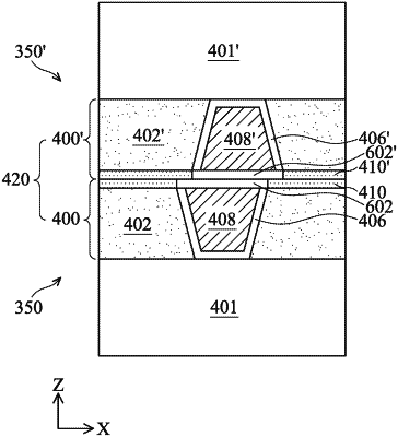
1. A method for forming an interfacial structure, comprising:
forming a first structure, comprising:
forming an opening in a dielectric layer;
forming a conductive feature in the opening;
selectively forming a first cap layer on the conductive feature by a first process; and then
selectively forming a first thermal conductive layer on the dielectric layer by a second process different from the first process, wherein a surface of the first thermal conductive layer and a surface of the first cap layer are substantially co-planar;
forming a second structure; and
bonding the second structure to the first structure.