| CPC H01L 27/0248 (2013.01) [H01L 27/0262 (2013.01)] | 20 Claims |

|
1. An integrated circuit comprising:
a first semiconductor device including:
a first N type well located in a substrate;
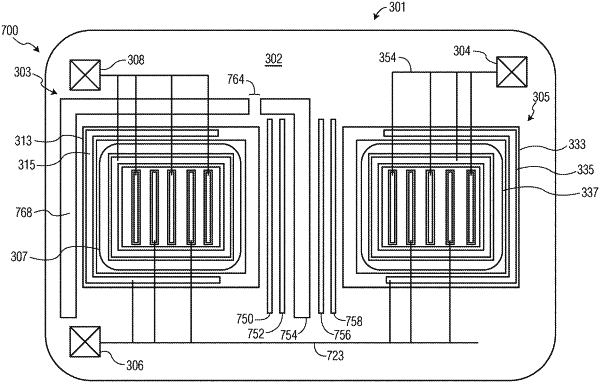
a first P type region located in the substrate and located at least on a first lateral side of the first N type well and at least partially surrounding the first N type well;
a second semiconductor device that is characterized as an ESD device, the second semiconductor device including:
a second N type well located in the substrate spaced apart from the first N type well;
wherein the substrate includes a first area on a second lateral side of the first N type well opposite to the first lateral side, the first area is located in a corresponding area to an area of the first P type region on the first lateral side of the first N type well, wherein the first N type well is located laterally between the first area and the area of the first P type region on the first lateral side of the first N type well, wherein the second lateral side of first N type well is a closest lateral side to the second N type well;
a conductivity reduction feature that provides a greater resistivity in at least a portion of a current path from a first integrated circuit terminal to the first area than in a current path from the first integrated circuit terminal to the first P type region located on the first lateral side of the first N type well;
a first conductive tie biasing structure located directly over an N type region of the substrate and directly over a P type region of the substrate at a second area of the substrate that is located directly laterally between the first area and the second N type well, the first conductive tie biasing structure electrically connects the N type region and the P type region of which it is located directly over;
a second conductive tie biasing structure located directly over an N type region of the substrate and directly over an P type region of the substrate at a third area of the substrate, the first P type region is located directly laterally between the third area and the first N type well, the second conductive tie biasing structure electrically connects the N type region and the P type region of which it is located directly over;
wherein the first conductive tie biasing structure and the second conductive tie biasing structure are not electrically connected to each other and are not electrically coupled to each other by a conductive biasing structure.
|