| CPC H01L 24/83 (2013.01) [H01L 24/32 (2013.01); H01L 25/0657 (2013.01); H01L 25/50 (2013.01); H01L 2224/32145 (2013.01); H01L 2224/83896 (2013.01); H01L 2924/05042 (2013.01); H01L 2924/0509 (2013.01); H01L 2924/05442 (2013.01); H01L 2924/0549 (2013.01)] | 20 Claims |
|
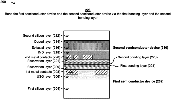
1. A method, comprising:
forming a first bonding layer on a surface of a first semiconductor device;
forming a second bonding layer on a surface of a second semiconductor device,
wherein a chemical composition of the first bonding layer is different from a chemical composition of the second bonding layer to promote bonding between the first semiconductor device and the second semiconductor device, wherein the chemical composition of the first bonding layer comprises a hydroxy-containing silicon dioxide; and
performing an annealing operation to bond the first semiconductor device with the second semiconductor device via the first bonding layer and the second bonding layer.
|