| CPC H01L 24/17 (2013.01) [H01L 21/4853 (2013.01); H01L 21/486 (2013.01); H01L 21/563 (2013.01); H01L 21/565 (2013.01); H01L 21/6835 (2013.01); H01L 23/3128 (2013.01); H01L 23/3135 (2013.01); H01L 23/49827 (2013.01); H01L 23/49838 (2013.01); H01L 23/562 (2013.01); H01L 24/08 (2013.01); H01L 24/16 (2013.01); H01L 24/80 (2013.01); H01L 25/0655 (2013.01); H01L 25/50 (2013.01); H01L 2221/68331 (2013.01); H01L 2224/08225 (2013.01); H01L 2224/16227 (2013.01); H01L 2224/17517 (2013.01); H01L 2224/80895 (2013.01); H01L 2224/80896 (2013.01); H01L 2924/3511 (2013.01)] | 20 Claims |
|
19. A package comprising:
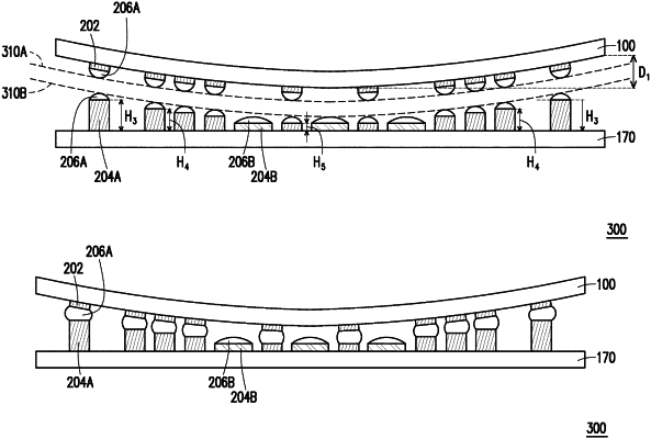
a first integrated circuit device attached to a first side of an interposer with a first set of connectors, the first set of connectors having a same height;
a die package attached to the first side of the interposer with a second set of connectors, the second set of connectors having multiple heights, a first set of dummy connectors being between the interposer and the die package, the first set of dummy connectors being electrically isolated from the die package and the first integrated circuit device, at least one of the first set of dummy connectors being between connectors of the second set of connectors;
an underfill on the first side of the interposer beneath the first integrated circuit device and the die package; and
an encapsulant surrounding the first integrated circuit device and the die package.
|