| CPC H01L 23/562 (2013.01) [H01L 21/76804 (2013.01); H01L 23/5384 (2013.01); H01L 23/5386 (2013.01)] | 11 Claims |
|
1. A method for fabricating an electronic package, comprising:
providing a plurality of electronic elements;
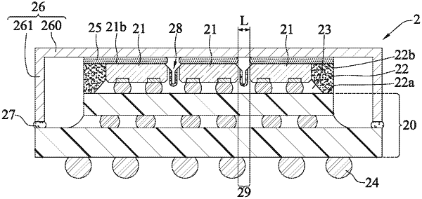
forming a spacing structure between any adjacent two of the plurality of electronic elements for connecting the adjacent two of the electronic elements, wherein a filling material and an encapsulant constitute the spacing structure, wherein the filling material is formed between the adjacent two of the plurality of electronic elements, the filling material is in contact with opposing side surfaces of the adjacent two of the plurality of electronic elements, and a first recess is formed within the filling material, and wherein the encapsulant is formed in the first recess, and a second recess is formed within the encapsulant;
and
providing a plurality of conductive elements electrically connected to the plurality of electronic elements to serve as external contacts.
|