| CPC H01L 23/5286 (2013.01) [G06F 30/392 (2020.01); G06F 30/3953 (2020.01); G06F 2119/06 (2020.01)] | 20 Claims |

|
1. A method of manufacturing a semiconductor device, comprising:
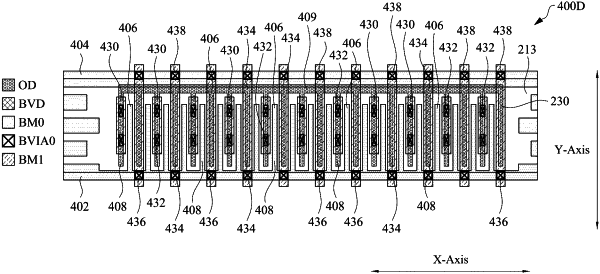
forming active regions on a semiconductor substrate, wherein each active region of the active regions has a long axis that extends in a first direction;
forming a first buried conductive rail having a long axis that extends in the first direction;
forming a first set of buried conductive fingers that extends from the first buried conductive rail;
each buried conductive finger in the first set of buried conductive fingers having a long axis that extends in a second direction, the second direction being substantially orthogonal to the first direction; and
the first set of buried conductive fingers extending beneath more than one of the active regions; and
forming a second set of buried conductive fingers;
each buried conductive finger in the second set of buried conductive fingers having a long axis that extends in the second direction;
the second set of buried conductive fingers extending beneath more than one of the active regions; and
the second set of buried conductive fingers being interleaved with the first set of buried conductive fingers.
|