| CPC H01L 23/528 (2013.01) [H01L 21/76814 (2013.01); H01L 21/76831 (2013.01); H01L 21/76843 (2013.01)] | 8 Claims |
|
1. A method for forming a semiconductor structure, comprising:
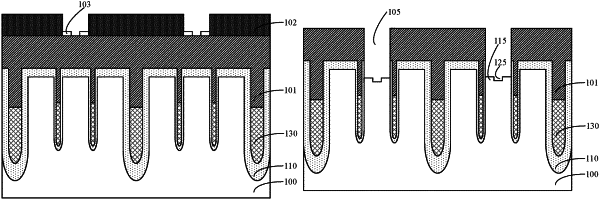
providing a substrate, and forming a dielectric layer on a surface of the substrate;
forming a mask layer on a surface of the dielectric layer, wherein the mask layer is arranged with a first opening penetrating the mask layer in a thickness direction of the mask layer;
forming a first barrier layer on a sidewall of the first opening, wherein the first barrier layer surrounds and forms a second opening;
forming a second barrier layer filling the second opening;
removing the first barrier layer and the second barrier layer by a first etching process until the first barrier layer or the second barrier layer is completely removed, wherein a removed rate of the first barrier layer by the first etching process is different from a removed rate of the second barrier layer by the first etching process; and
removing the dielectric layer exposed by the first opening and part of the substrate exposed by the first opening, to form a bit-line contact opening, wherein a bottom of the bit-line contact opening is arranged with a convex region and a concave region, and the convex region and the concave region have a height difference;
wherein, the convex region surrounds the concave region, or, the concave region surrounds the convex region;
wherein the removing the first barrier layer and the second barrier layer by a first etching process until the first barrier layer or the second barrier layer is completely removed comprises:
removing the first barrier layer and the second barrier layer by the first etching process until one of the first barrier layer and the second barrier layer with a faster etched rate is completely removed;
wherein the removing the first barrier layer and the second barrier layer by the first etching process until one of the first barrier layer and the second barrier layer with a faster etched rate is completely removed comprises:
removing the dielectric layer exposed by the first opening and part of the substrate exposed by the first opening to form a bit-line contact opening, comprising:
etching a remaining first barrier layer or a remaining second barrier layer by a second etching process, and etching the dielectric layer exposed by the first opening until the substrate is exposed; and
etching the substrate by a preset thickness by a third etching process to form the bit-line contact opening, wherein the substrate to-be-etched is exposed by the first opening.
|