US 12,205,888 B2
Semiconductor packages and methods of forming the same
Ching-Yu Huang, Hsinchu (TW); Han-Ping Pu, Taichung (TW); Ming-Kai Liu, Hsinchu (TW); Ting-Chu Ko, Hsinchu (TW); Yung-Ping Chiang, Hsinchu County (TW); Chang-Wen Huang, Hsinchu (TW); and Yu-Sheng Hsieh, New Taipei (TW)
Assigned to Taiwan Semiconductor Manufacturing Company, Ltd, Hsinchu (TW)
Filed by Taiwan Semiconductor Manufacturing Company, Ltd., Hsinchu (TW)
Filed on Aug. 1, 2023, as Appl. No. 18/363,692.
Application 17/382,371 is a division of application No. 16/035,723, filed on Jul. 16, 2018, granted, now 11,075,159, issued on Jul. 27, 2021.
Application 18/363,692 is a continuation of application No. 17/382,371, filed on Jul. 22, 2021, granted, now 11,929,319.
Prior Publication US 2023/0378058 A1, Nov. 23, 2023
This patent is subject to a terminal disclaimer.
Int. Cl. H01L 23/00 (2006.01); H01L 21/56 (2006.01); H01L 21/768 (2006.01); H01L 23/31 (2006.01); H01L 23/522 (2006.01); H01L 23/532 (2006.01); H01L 23/538 (2006.01)
CPC H01L 23/5226 (2013.01) [H01L 21/56 (2013.01); H01L 21/76873 (2013.01); H01L 23/3157 (2013.01); H01L 23/53238 (2013.01); H01L 23/5381 (2013.01); H01L 23/5383 (2013.01); H01L 24/09 (2013.01); H01L 24/14 (2013.01); H01L 2224/02379 (2013.01); H01L 2224/0401 (2013.01)] 20 Claims
OG exemplary drawing
 
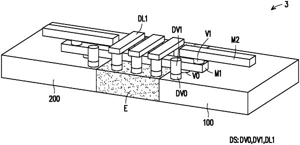
1. A semiconductor package, comprising:
two dies, laterally disposed side by side;
an encapsulant, disposed between the two dies;
a first metal line, disposed over the two dies and across the encapsulant between the two dies; and
a plurality of dummy vias, disposed aside the first metal line,
wherein some of the dummy vias are in physical contact with the encapsulant.