US 12,205,859 B2
Package and printed circuit board attachment
Pei-Haw Tsao, Tai-chung (TW); Tsung-Hsing Lu, Jhubei (TW); and Li-Huan Chu, Hsinchu (TW)
Assigned to TAIWAN SEMICONDUCTOR MANUFACTURING CO., LTD., Hsinchu (TW)
Filed by Taiwan Semiconductor Manufacturing Co., Ltd., Hsinchu (TW)
Filed on Mar. 20, 2023, as Appl. No. 18/186,310.
Application 16/685,337 is a division of application No. 16/036,544, filed on Jul. 16, 2018, granted, now 10,510,633, issued on Dec. 17, 2019.
Application 18/186,310 is a continuation of application No. 17/120,758, filed on Dec. 14, 2020, granted, now 11,610,827.
Application 17/120,758 is a continuation of application No. 16/685,337, filed on Nov. 15, 2019, granted, now 10,867,881, issued on Dec. 15, 2020.
Prior Publication US 2023/0230891 A1, Jul. 20, 2023
Int. Cl. H01L 23/31 (2006.01); H01L 23/00 (2006.01); H01L 23/14 (2006.01); H01L 23/498 (2006.01); H05K 1/11 (2006.01)
CPC H01L 23/3128 (2013.01) [H01L 23/142 (2013.01); H01L 23/3114 (2013.01); H01L 23/49816 (2013.01); H01L 23/49827 (2013.01); H01L 24/10 (2013.01); H05K 1/111 (2013.01)] 20 Claims
OG exemplary drawing
 
1. A method of forming a semiconductor device structure, the method comprising:
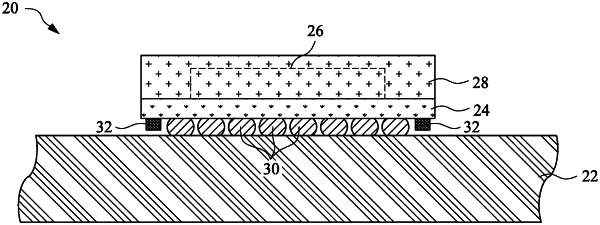
attaching a plurality of pins to a first substrate, the first substrate comprising a first plurality of pads, the plurality of pins being attached to a first subset of the first plurality of pads, wherein the pins of the plurality of pins are discontinuous and spaced apart from each other; and
attaching the first substrate to a second substrate, the second substrate comprising a second plurality of pads, the second plurality of pads being electrically coupled to a second subset of the first plurality of pads, wherein the plurality of pins is between the first substrate and the second substrate.