| CPC H01L 22/32 (2013.01) [H01L 22/20 (2013.01); H01L 23/544 (2013.01); H01L 24/03 (2013.01); H01L 24/08 (2013.01)] | 20 Claims |
|
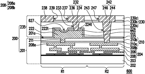
1. A semiconductor structure, comprising:
a first die comprising an interconnect structure and a pad structure disposed on and electrically connected to the interconnect structure, wherein the pad structure comprises a metal pad and a dielectric cap on the metal pad, and the pad structure has a first probe mark recessed from a top surface of the dielectric cap into a top surface of the metal pad, wherein the first probe mark extends from the top surface of the dielectric cap, via a sidewall of the dielectric cap, onto the top surface of the metal pad, and the sidewall of the dielectric cap is connected to the top surface of the dielectric cap being recessed therefrom;
a protective layer conformally covering the pad structure, wherein the protective layer is in contact with the probe mark; and
a first bonding structure disposed on the first die, wherein the first bonding structure at least comprises a first bonding metal layer penetrating through the protective layer and the dielectric cap to contact the pad structure having the first probe mark.
|