| CPC H01L 22/14 (2013.01) [H01L 22/20 (2013.01); H01L 24/03 (2013.01); H01L 24/05 (2013.01); H01L 24/08 (2013.01); H01L 24/13 (2013.01); H01L 24/32 (2013.01); H01L 2224/03001 (2013.01); H01L 2224/0392 (2013.01); H01L 2224/0401 (2013.01); H01L 2224/05073 (2013.01); H01L 2224/05082 (2013.01); H01L 2224/05083 (2013.01); H01L 2224/05084 (2013.01); H01L 2224/05124 (2013.01); H01L 2224/05147 (2013.01); H01L 2224/05166 (2013.01); H01L 2224/05564 (2013.01); H01L 2224/05573 (2013.01); H01L 2224/05647 (2013.01); H01L 2224/05655 (2013.01); H01L 2224/05666 (2013.01); H01L 2224/05686 (2013.01); H01L 2224/08145 (2013.01); H01L 2224/13007 (2013.01); H01L 2224/32145 (2013.01)] | 20 Claims |
|
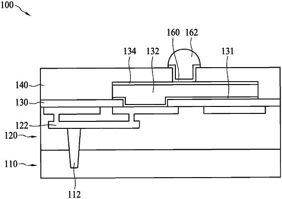
1. A semiconductor device comprising:
a semiconductor die that includes a device layer, an interconnect layer over the device layer, a conductive pad over the interconnect layer, a conductive seed layer directly on the conductive pad, and a passivation layer encapsulating the conductive pad and the conductive seed layer, wherein the conductive pad is between the interconnect layer and the conductive seed layer, wherein a conductive feature lands on the conductive pad and is free from a physical interface with the conductive seed layer, wherein the conductive seed layer is smaller than the conductive pad from a top view.
|