| CPC H01L 22/14 (2013.01) [G01R 31/2896 (2013.01); G01R 31/318513 (2013.01); G11C 14/0018 (2013.01); H01L 23/31 (2013.01); H01L 25/0657 (2013.01)] | 15 Claims |
|
1. A method of manufacturing a multi-chip package (MCP) comprising a first type semiconductor chip and a second type semiconductor chip, the method comprising:
mounting the first type semiconductor chip on a substrate;
mounting the second type semiconductor chip on the first type semiconductor chip;
mounting a third type semiconductor chip on the substrate;
forming a mold layer to cover the first and second type semiconductor chips;
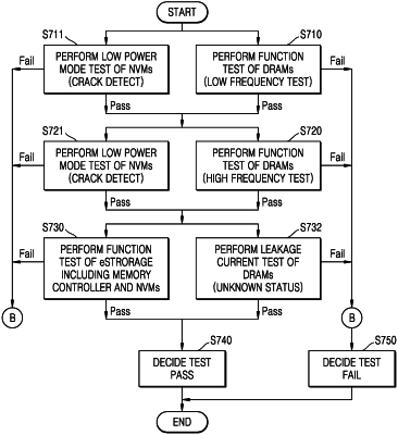
placing the MCP on test equipment, wherein the test equipment comprises a test host configured to test the MCP;
performing a function test on the first type semiconductor chip using first channel terminals of the test equipment, wherein the test host applies signals related to the function test of the first type semiconductor chip to the first channel terminals;
performing a low power mode test on the second type semiconductor chip using second channel terminals of the test equipment, wherein the test host applies signals related to the low power mode test of the second type semiconductor chip to the second channel terminals;
measuring current flowing through the second channel terminals in the low power mode test of the second type semiconductor chip;
analyzing a current measured in the second channel terminals to determine if a crack defect exists in the second type semiconductor chip; and
to make the second type semiconductor chip entering the low power mode test:
applying by the test host, a hardware reset signal RST_n having a ground voltage to a channel terminal connected to the third type semiconductor chip among the second channel terminals, and
transmitting a chip enable signal nCE having a high level to the second type semiconductor chip from the third type semiconductor chip,
wherein the function test of the first type semiconductor chip and the low power mode test of the second type semiconductor chip are performed in parallel, and
wherein in the low power mode test of the second type semiconductor chip, the second type semiconductor chip has a limited current load that flows a limited current through the second type semiconductor chip.
|