| CPC H01L 21/30604 (2013.01) [H01L 21/31053 (2013.01); H01L 21/31144 (2013.01); H01L 29/0665 (2013.01); H01L 29/0673 (2013.01); H01L 29/42392 (2013.01)] | 20 Claims |
|
1. A method of forming a semiconductor device, comprising:
forming a nanostructure having a first set of layers of a first material and a second set of layers, alternating with the first set of layers, having a second material;
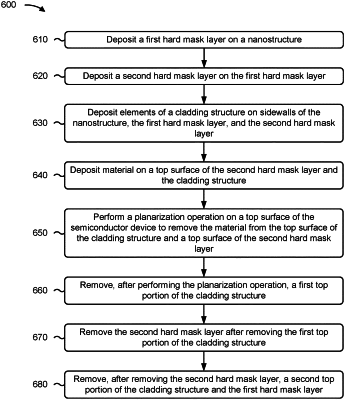
depositing a hard mask on a top layer of the first set of layers, the hard mask including a first hard mask layer on the top layer of the first set of layers and a second hard mask layer on the first hard mask layer;
depositing elements of a cladding structure, comprising a silicon germanium-based material, on sidewalls of the nanostructure and the hard mask;
removing a top portion of the cladding structure; and
removing the second hard mask layer after removing the top portion of the cladding structure.
|