| CPC H01L 21/0337 (2013.01) [C23C 16/38 (2013.01); H01L 21/0332 (2013.01)] | 18 Claims |
|
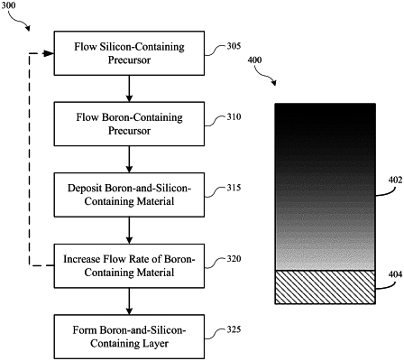
1. A semiconductor processing method comprising:
flowing a silicon-containing precursor into a substrate processing region of a semiconductor processing chamber;
flowing a boron-containing precursor into the substrate processing region of the semiconductor processing chamber; and
depositing a boron-and-silicon-containing layer on a substrate in the substrate processing region of the semiconductor processing chamber, wherein the boron-and-silicon-containing layer is characterized by a linearly increasing ratio of boron-to-silicon from a first surface in contact with the substrate to a second surface of the boron-and-silicon-containing layer opposite the first surface, and wherein a flow rate of the boron-containing precursor increases non-linearly during the deposition of the boron-and-silicon-containing layer.
|