| CPC G11C 7/1063 (2013.01) [G11C 5/06 (2013.01); G11C 7/1069 (2013.01); G11C 7/1096 (2013.01)] | 8 Claims |
|
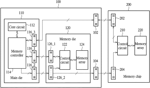
1. A multi-die package, comprising:
a main die comprising a memory controller, a first set of pads, a second set of pads and a third set of pads, wherein each of the first set of pads, the second set of pads and the third set of pads comprises a plurality of pads;
a memory die, coupled to the first set of pads and the second set of pads of the main die;
a first set of pins, coupled to the third set of pads of the main die; and
a second set of pins, coupled to the second set of pads of the main die;
wherein the memory controller accesses the memory die through the first set of pads and the second set of pads, and the memory controller accesses a memory chip external to the multi-die package through the second set of pads and the third set of pads;
wherein the memory controller transmits a command signal and an address signal to the memory die and the memory chip through the second set of pads; and the memory controller writes data into the memory die or reads data from the memory die through the first set of pads, or the memory controller writes data into the memory chip or reads data from the memory chip through the third set of pads;
wherein the memory controller determines whether to access only one of the memory die and the memory chip, or to access the memory die and the memory chip at a same time according to a bandwidth required by an application program executed by a core circuit in the main die.
|