| CPC G11C 16/10 (2013.01) [G11C 16/0483 (2013.01); G11C 16/08 (2013.01); H10B 41/27 (2023.02); H10B 43/27 (2023.02); G11C 11/5628 (2013.01); G11C 11/5671 (2013.01)] | 16 Claims |
|
1. A method of programming a memory device, comprising the steps of:
preparing a memory device that includes a plurality of memory cells, the plurality of memory cells being arranged in a plurality of word lines;
during a first program loop of a single bit per cell programming operation and then during a second program loop of a multi-bit per cell programming operation:
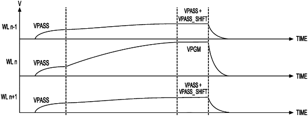
applying a first voltage to a control gate of a selected word line of the plurality of word lines, during a ramping period that lasts a first duration, gradually and continuously increasing a voltage that is applied to the control gate of the selected word line from the first voltage until the voltage that is applied to the control gate of the selected word line reaches only a single programming voltage,
holding the voltage applied to the control gate of the selected word line at the single programming voltage over a second duration that is less than the first duration, and
immediately after holding the voltage applied to the control gate of the selected word line at the single programming voltage, ramping the voltage applied to the control gate of the selected word line down from the single programming voltage.
|