| CPC G09G 3/3233 (2013.01) [G09G 3/2007 (2013.01); H10K 59/1213 (2023.02); G09G 2300/0819 (2013.01); G09G 2300/0842 (2013.01); G09G 2300/0852 (2013.01); G09G 2300/0861 (2013.01); G09G 2310/08 (2013.01); G09G 2320/0247 (2013.01); G09G 2320/0257 (2013.01); G09G 2330/021 (2013.01)] | 18 Claims |
|
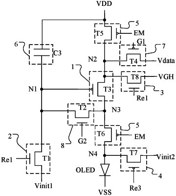
1. A pixel driving circuit, applied to a display panel, and comprising:
a driving transistor, wherein a gate of the driving transistor is coupled to a first node, a first electrode of the driving transistor is coupled to a second node, and a second electrode of the driving transistor is coupled to a third node;
a data write circuit, coupled to the second node and a data signal terminal, and configured to transmit a signal of the data signal terminal to the second node in response to a signal of a first gate driving signal terminal;
a threshold compensation circuit, coupled to the first node, the third node and a second gate driving signal terminal, and configured to communicate the first node with the third node in response to a signal of the second gate driving signal terminal;
a first capacitor, coupled between the first node and the first gate driving signal terminal; and
a second capacitor, coupled between the first node and the second gate driving signal terminal;
wherein a turn-on level of the data write circuit is a low level, a turn-on level of the threshold compensation circuit is a high level, and a capacitance value of the first capacitor is greater than a capacitance value of the second capacitor;
wherein the threshold compensation circuit comprises:
a N-type second transistor, wherein a gate of the N-type second transistor is coupled to a second gate line and a third gate line, a first electrode of the N-type second transistor is coupled to a gate of the driving transistor, and a second electrode of the N-type second transistor is coupled to a second electrode of the driving transistor, and wherein the second gate line and the third gate line are used to provide the second gate driving signal terminal;
wherein the data write circuit comprises:
a P-type fourth transistor, wherein a gate of the P-type fourth transistor is coupled to a first gate line, a first electrode of the P-type fourth transistor is coupled to a data line, and a second electrode of the P-type fourth transistor is coupled to a first electrode of the driving transistor, and wherein the first gate line is used to provide the first gate driving signal terminal, and the data line is used to provide the data signal terminal;
wherein a first electrode of the first capacitor is coupled to the first gate line, and a second electrode of the first capacitor is coupled to the gate of the driving transistor; and
wherein a first electrode of the second capacitor is coupled to the third gate line, and a second electrode of the second capacitor is coupled to the gate of the driving transistor;
wherein the display panel further comprises:
a base substrate;
a first conductive layer, located on a side of the base substrate, and comprising a first conductive portion and the first gate line, wherein the first conductive portion is used to form the gate of the driving transistor, and an orthographic projection of the first gate line on the base substrate is extended along a first direction;
a second conductive layer, located on a side of the first conductive layer away from the base substrate, and comprising the second gate line, wherein an orthographic projection of the second gate line on the base substrate is extended along the first direction;
a second active layer, located on a side of the second conductive layer away from the base substrate, and comprising a first active portion and a third active portion coupled to each other, wherein the first active portion is used to form a channel region of the second transistor, and an orthographic projection of the first active portion on the base substrate is covered by an orthographic projection of the second gate line on the base substrate;
a third conductive layer, located on a side of the second active layer away from the base substrate, and comprising the third gate line, wherein an orthographic projection of the third gate line on the base substrate is extended along with the first direction, and the orthographic projection of the first active portion on the base substrate is covered by the orthographic projection of the third gate line on the base substrate; and
a fourth conductive layer, located on a side of the third conductive layer away from the base substrate, and comprising a connection portion, wherein the connection portion is coupled to the first conductive portion and the third active portion through via holes, respectively;
wherein the first gate line comprises a first extension portion, an orthographic projection of the first extension portion on the base substrate is coincided with an orthographic projection of the third active portion on the base substrate, the first extension portion is used to form the first electrode of the first capacitor, and the third active portion is used to form the second electrode of the first capacitor; and
the third gate line comprises a third extension portion, the connection portion comprises a fourth extension portion, an orthographic projection of the third extension portion on the base substrate is coincided with an orthographic projection of the fourth extension portion on the base substrate, the first electrode of the second capacitor comprises the third extension portion, and the second electrode of the second capacitor comprises the fourth extension portion.
|