| CPC G06F 1/1656 (2013.01) [B41M 1/34 (2013.01); B41M 3/003 (2013.01); G02B 1/04 (2013.01); G02B 1/14 (2015.01)] | 15 Claims |
|
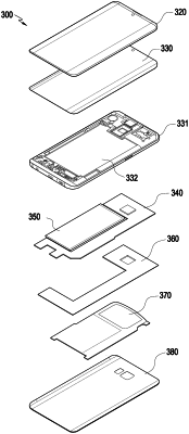
1. An electronic device comprising:
a housing comprising a translucent ceramic member; and
a printing film provided on the housing,
wherein the printing film comprises:
an adhesive layer provided on the ceramic member;
a base layer comprising a first surface facing the adhesive layer and a second surface opposite to the first surface;
a printing layer provided on the first surface of the base layer, the printing layer being viewable through the ceramic member and the adhesive layer; and
a shielding printing layer facing the second surface of the base layer.
|