| CPC G02F 1/136286 (2013.01) [G02F 1/1339 (2013.01); G02F 1/136209 (2013.01); G02F 1/136222 (2021.01); G02F 1/1368 (2013.01)] | 15 Claims |
|
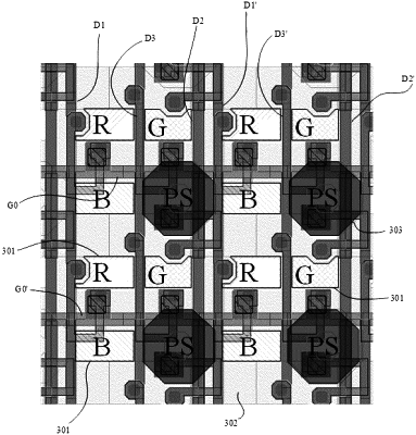
1. A display substrate, comprising a plurality of pixel regions each corresponding to a pixel, wherein each pixel region comprises sub-regions in at least two rows, the sub-regions in each row comprise at least two sub-regions, a part of the sub-regions in each pixel region correspond to sub-pixels of the pixel, and at least one of the sub-regions is an opaque region;
wherein the display substrate is an array substrate, and the array substrate comprises a second base substrate and a plurality of scanning lines, a plurality of data lines and a pixel driving circuitry arranged on the second base substrate;
the plurality of scanning lines extends along a first direction and is arranged along a second direction on the second base substrate, the plurality of data lines extends along the second direction and is arranged along the first direction on the second base substrate, and the first direction intersects the second direction; and
the pixel driving circuitry is electrically coupled to the scanning line and the data line, the pixel driving circuitry comprises a sub-pixel driving circuitry corresponding to each sub-pixel, the sub-pixel driving circuitry is configured to drive a corresponding sub-pixel, and the scanning lines, or the data lines, or the scanning lines and the data lines, coupled to the sub-pixel driving circuitry corresponding to the sub-pixels in different colors in each pixel are different;
wherein the sub-pixels in each pixel correspond to a same scanning line and different data lines:
wherein the pixel region corresponding to each pixel comprises four sub-regions arranged in two rows and two columns, three of the four sub-regions correspond to the sub-pixels in different colors respectively, and the other one of the four sub-regions is the opaque region;
three data lines correspond to each pixel, and the three data lines comprise a first data line, a second data line, and a third data line; and
the first data line is located at an edge of the pixel region away from the opaque region along the first direction, the second data line is located at an edge of the pixel region close to the opaque region along the first direction, and the third data line is located in the middle of the pixel region along the first direction and at a side close to the opaque region;
wherein an orthogonal projection of the opaque region onto the second base substrate overlaps with orthogonal projections of the second data line and the third data line onto the second base substrate, and the orthogonal projection of the opaque region onto the second base substrate overlaps with an orthogonal projection of the first data line for the pixel regions in a next column in the first direction onto the second base substrate;
wherein one scanning line corresponds to each pixel, and the scanning line is located in the middle of the pixel region and at a side close to the opaque region;
wherein the scanning line comprises a first portion extending along the first direction and a second portion, an end of the second portion is coupled to the first portion, the other end of the second portion extends to a side of the pixel region close to the opaque region along the second direction, and the second portion is used as a gate electrode of a thin film transistor of a sub-pixel in a same row as the opaque region along the first direction; and
wherein the orthogonal projection of the opaque region onto the second base substrate overlaps with an orthogonal projection of the first portion onto the second base substrate and an orthogonal projection of the second portion onto the second base substrate.
|