| CPC G02F 1/1339 (2013.01) [G02F 1/133354 (2021.01); G02F 1/1337 (2013.01); G02F 1/134345 (2021.01); G02F 1/133345 (2013.01); G02F 2201/07 (2013.01); H01L 27/1218 (2013.01); H01L 27/124 (2013.01)] | 19 Claims |
|
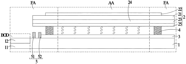
1. A display panel having a display area and a non-display area adjacent to the display area, wherein the display panel comprises:
an array substrate on which a bonding electrode is arranged, wherein the bonding electrode is located in the non-display area;
an opposite substrate, arranged opposite to the array substrate;
a first alignment film, arranged on a side of the array substrate close to the opposite substrate; and
a retaining wall structure, arranged on the side of the array substrate close to the opposite substrate, wherein at least a part of the retaining wall structure is located between the first alignment film and the bonding electrode,
wherein the array substrate in the non-display area comprises:
a first base substrate;
a buffer layer, arranged on a side of the first base substrate;
a bonding lead, arranged on a side of the buffer layer away from the first base substrate; and
an insulating layer group, arranged on a side of the bonding lead away from the first base substrate, wherein the insulating layer group is provided with a notch, so that the bonding lead is exposed to form the bonding electrode.
|