| CPC H10K 59/122 (2023.02) [H10K 59/353 (2023.02)] | 19 Claims |

|
1. A display device comprising:
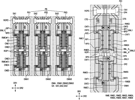
subpixels each comprising an emission area;
electrodes which are disposed in the emission area, extend in a first direction, and are spaced apart in a second direction intersecting the first direction;
a first insulating layer disposed on the electrodes;
a first bank comprising:
a first bank part disposed on the first insulating layer and surrounding the emission area; and
a second bank part connected to the first bank part and disposed in the emission area;
light emitting elements disposed on the electrodes spaced apart in the second direction, wherein a height of the second bank part of the first bank is lower than a height of the first bank part of the first bank;
a second insulating layer which is dispose on the light emitting elements and the second bank part and exposes ends of each of the light emitting elements; and
contact electrodes which are disposed on the electrodes and the second insulating layer and contact the light emitting elements.
|