| CPC H10K 50/8428 (2023.02) [H01L 33/52 (2013.01); H10K 50/844 (2023.02); H10K 50/8423 (2023.02); H10K 50/8426 (2023.02); H10K 71/00 (2023.02)] | 14 Claims |

|
1. A display device comprising:
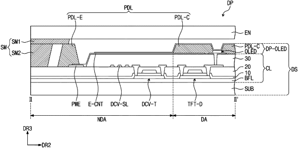
a display substrate comprising a base substrate including a display area and a non-display area, a circuit layer on the base substrate, light emitting elements on the circuit layer and overlapping the display area, and a pixel defining layer on the circuit layer and in which openings corresponding to the light emitting elements are defined;
an encapsulation substrate over the display substrate; and
a sealing member coupling the display substrate and the encapsulation substrate and non-overlapping the display area,
wherein the pixel defining layer comprises an edge portion overlapping the non-display area, and a central portion overlapping the display area, the edge portion comprising an outer surface facing away from the display area, and
the sealing member comprises:
a first portion comprising an inner portion between the display substrate and the encapsulation substrate and overlapping the edge portion of the pixel defining layer, and an outer portion extending from the inner portion and located outside the inner portion; and
a second portion between the outer portion and the display substrate and spaced apart from the edge portion of the pixel defining layer,
wherein the first portion and the second portion define an interface,
wherein the sealing member is spaced from the outer surface of the edge portion of the pixel defining layer so as to define a gap therebetween along an outward direction extending from the display area toward the non-display area,
wherein the second portion comprises a material having an elastic modulus less than that of a material of the first portion, and
the first portion is adjacent to the encapsulation substrate, and the second portion is spaced apart from the encapsulation substrate.
|