| CPC H10B 43/35 (2023.02) [G11C 16/0466 (2013.01); H01L 29/40117 (2019.08); H01L 29/4234 (2013.01); H01L 29/6656 (2013.01); H01L 29/7881 (2013.01); H01L 29/7923 (2013.01); H10B 41/10 (2023.02); H10B 41/35 (2023.02); H10B 43/10 (2023.02)] | 16 Claims |

|
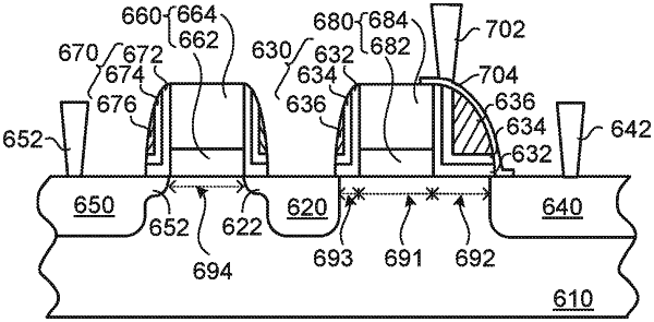
1. A memory cell of a non-volatile memory, the memory cell comprising a memory element, the memory element comprising:
a well region;
a gate structure formed on a surface of the well region, wherein the gate structure comprises at least one protrusion part;
a spacer arranged around a sidewall of the gate structure and contacted with the surface of the well region, wherein the spacer comprises a first part and a second part; and
a first doped region and a second doped region formed under the surface of the well region, wherein a region between the first doped region and the second doped region is a channel region, and the channel region comprises a first channel and a second channel,
wherein the first part of the spacer is arranged around the at least one protrusion part, and a width of the first part of the spacer is wider than a width of the second part of the spacer, and the width of the first part of the spacer is smaller than or equal to three times the width of the second part of the spacer,
wherein both of the first part of the spacer and the second part of the spacer comprise a first silicon oxide layer, a silicon nitride layer and a second silicon oxide layer, wherein the first silicon oxide layer is contacted with the surface of the well region and the sidewall of the gate structure, the silicon nitride layer covers the first silicon oxide layer, and the second silicon oxide layer covers the silicon nitride layer, wherein the silicon nitride layer is a charge-trapping layer,
wherein the sidewall of the gate structure comprises plural surfaces, and a first surface of the at least one protrusion part is in parallel with a length direction of the channel region,
wherein the first channel is located under the gate structure, the second channel is arranged between the first channel and the second doped region, and the first part of the spacer is located over the second channel,
wherein when a program operation is performed, the gate structure receives a gate voltage and plural carriers are injected into the charge-trapping layer in the first part of the spacer through the second channel.
|
|
9. A memory cell of a non-volatile memory, the memory cell comprising:
a memory element comprising a well region, a first gate structure, a first spacer, a first doped region and a second doped region; wherein the first gate structure is formed on a surface of the well region and the gate structure comprises at least one protrusion part, the first spacer is arranged around a sidewall of the first gate structure and contacted with the surface of the well region, the first spacer comprises a first part and a second part; wherein the first doped region and the second doped region are formed under the surface of the well region, a region between the first doped region and the second doped region is a channel region, and the channel region comprises a first channel and a second channel; wherein the sidewall of the gate structure comprises plural surfaces, and a first surface of the at least one protrusion part is in parallel with a length direction of the channel region; wherein the first channel is located under the first gate structure, the second channel is arranged between the first channel and the second doped region, and the first part of the first spacer is located over the second channel; and
a select transistor comprising the well region, a second gate structure, a second spacer and a third doped region, wherein the second gate structure is formed on the surface of the well region, the second spacer is arranged around a sidewall of the second gate structure and contacted with the surface of the well region, and the third doped region is formed under the surface of the well region, wherein a region between the first doped region and third doped region is a fourth channel, and the fourth channel is located under the second gate structure,
wherein the first part of the first spacer is arranged around the at least one protrusion part, and a width of the first part of the first spacer is wider than a width of the second part of the first spacer, and the width of the first part of the first spacer is smaller than or equal to three times the width of the second part of the first spacer,
wherein both of the first part of the first spacer and the second part of the first spacer comprise a first silicon oxide layer, a silicon nitride layer and a second silicon oxide layer, wherein the first silicon oxide layer is contacted with the surface of the well region and the sidewall of the first gate structure, the silicon nitride layer covers the first silicon oxide layer, and the second silicon oxide layer covers the silicon nitride layer, wherein the silicon nitride layer is a charge-trapping layer,
wherein when a program operation is performed, the gate structure receives a gate voltage and plural carriers are injected into the charge-trapping layer in the first part of the first spacer through the second channel of the memory element.
|