| CPC H10B 43/27 (2023.02) [H01L 23/5226 (2013.01); H10B 41/10 (2023.02); H10B 41/27 (2023.02); H10B 41/40 (2023.02); H10B 43/10 (2023.02); H10B 43/40 (2023.02)] | 18 Claims |

|
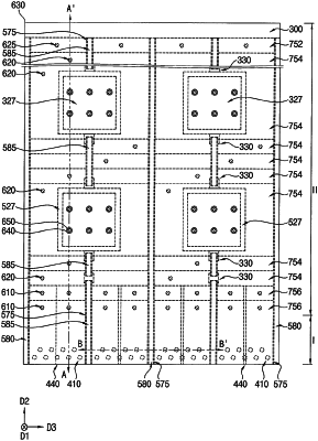
1. A vertical memory device comprising:
a gate electrode structure including gate electrodes spaced apart from each other on a substrate in a first direction substantially perpendicular to an upper surface of the substrate, each of the gate electrodes extending in a second direction substantially parallel to the upper surface of the substrate;
a channel extending in the first direction through the gate electrode structure;
an insulation pattern structure extending through the gate electrode structure;
an etch stop structure extending through the gate electrode structure and surrounding at least a portion of a sidewall of the insulation pattern structure, the etch stop structure including a filling pattern and an etch stop pattern on a sidewall of the filling pattern;
a through via extending in the first direction through the insulation pattern structure;
a first division pattern at each of opposite sides of the gate electrode structure in a third direction substantially parallel to the upper surface of the substrate and crossing the second direction, each of the first division pattern extending in the second direction; and
second division patterns spaced apart from each other in the second direction between the first division patterns, each of the second division patterns extending through the gate electrode structure,
wherein an upper surface of each of the first and second division patterns is higher than an upper surface of the etch stop structure.
|