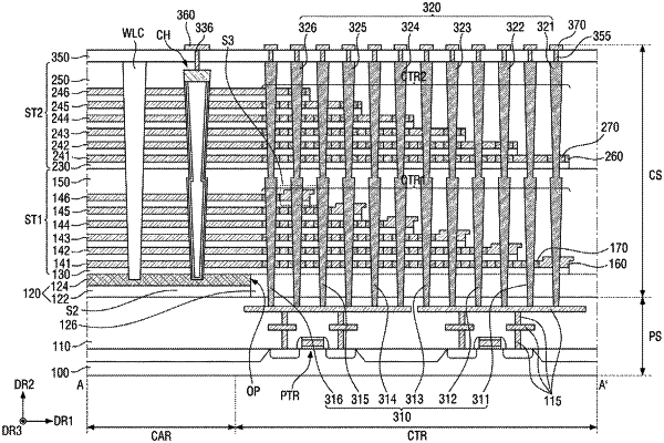
| CPC H10B 43/27 (2023.02) [H01L 23/5226 (2013.01); H10B 41/10 (2023.02); H10B 41/27 (2023.02); H10B 41/40 (2023.02); H10B 43/10 (2023.02); H10B 43/40 (2023.02)] | 20 Claims |

|
1. A semiconductor memory device comprising:
a first stacked structure on a substrate, the first stacked structure including a cell region and a first staircase portion extending in a first direction;
a second stacked structure on the first stacked structure, the second stacked structure including a second staircase portion extending in the first direction, the second staircase portion at least partially overlapping the first staircase portion in a second direction;
a first contact plug on the first staircase portion and the second staircase portion, the first contact plug penetrating the first stacked structure and the second stacked structure and extending in the second direction, wherein the first contact plug is electrically connected to the first stacked structure, and is not electrically connected to the second stacked structure; and
a second contact plug on the first staircase portion and the second staircase portion, the second contact plug penetrating the first stacked structure and the second stacked structure and extending in the second direction, wherein the second contact plug is electrically connected to the second stacked structure, and is not electrically connected to the first stacked structure.
|