| CPC H10B 41/42 (2023.02) [H01L 29/66825 (2013.01); H01L 29/7883 (2013.01); H10B 41/30 (2023.02)] | 20 Claims |

|
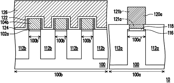
1. A manufacturing method of a semiconductor structure, comprising:
providing a substrate having a peripheral region and a memory region;
forming a plurality of first isolation structures in the substrate in the peripheral region, so that a first active area is defined between the first isolation structures;
forming an oxide layer on the substrate in the first active area, wherein a top surface of the oxide layer is covered by the first isolation structures, and an opening is defined in the oxide layer and the first isolation structures covering the oxide layer and exposes a part of the substrate; and
forming a gate structure on the substrate in the first active area, wherein steps of forming the gate structure comprises:
forming a gate dielectric layer on the substrate in the opening, so that the oxide layer is located around the gate dielectric layer; and
forming a gate on the gate dielectric layer, wherein a width of a bottom surface of the gate is less than a width of a top surface of the first active area.
|