| CPC H10B 12/485 (2023.02) [H10B 12/37 (2023.02)] | 13 Claims |

|
1. A semiconductor device comprising:
a substrate including an element separation film and an active region defined by the element separation film;
an insulating pattern on the substrate;
a bit line structure on the substrate;
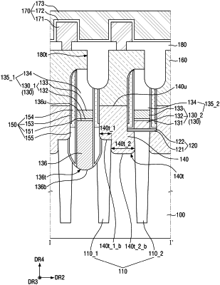
a trench in the element separation film and the active region, the trench on at least one side of the bit line structure and including a first portion in the element separation film and a second portion in the active region, a bottom face of the first portion placed above a bottom face of the second portion;
a single crystal storage contact including a first contact portion filling the first portion of the trench and a second contact portion filing the second portion of the trench, without a void; and
an information storage element electrically connected to the single crystal storage contact,
wherein the bit line structure includes a first bit line structure on the active region and across the single crystal storage contact, and a second bit line structure on the insulating pattern,
wherein a top face of the second contact portion is in contact with a bottom face of the insulating pattern,
wherein the bit line structure includes at least one of conductive film, and
wherein the single crystal storage contact entirely fills a part of the trench, the part of the trench overlapping the at least one of conductive film of the bit line structure in a direction parallel to an upper face of the substrate.
|