| CPC H10B 12/0335 (2023.02) [H01L 21/28568 (2013.01); H01L 21/7684 (2013.01); H01L 21/7685 (2013.01); H01L 21/76831 (2013.01); H01L 21/76876 (2013.01); H01L 21/76877 (2013.01); H01L 23/528 (2013.01); H01L 23/5226 (2013.01); H01L 23/53266 (2013.01); H01L 28/91 (2013.01); H10B 12/31 (2023.02); H10B 12/315 (2023.02); H01L 21/0217 (2013.01); H01L 21/0228 (2013.01)] | 5 Claims |
|
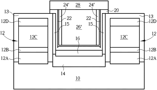
1. A storage node contact structure of a memory device, comprising:
a substrate having a dielectric layer, the dielectric comprises a recess;
a first tungsten metal layer disposed in the recess and filling the recess;
a spacer, disposed beside the first tungsten metal layer and directly contacts the first tungsten metal layer, wherein the spacer does not contact a bottom surface of the first tungsten metal layer directly;
a second tungsten metal layer disposed on the first tungsten metal layer, wherein the second tungsten metal layer is formed by a physical vapor deposition (PVD) method; and
an adhesive layer disposed between the first tungsten metal layer and the second tungsten metal layer, wherein a material of the adhesive layer comprises titanium or tantalum, wherein the adhesive layer directly contacts a top surface of the dielectric layer, wherein a width of the adhesive layer is same as a width of the second tungsten metal layer, and the width of the adhesive layer is larger than a width of the first tungsten metal layer.
|