| CPC H05K 5/065 (2013.01) [H05K 1/0218 (2013.01); H05K 7/02 (2013.01); H05K 9/0088 (2013.01); H05K 2201/0723 (2013.01)] | 20 Claims |
|
1. A printed circuit board assembly (PCBA) device, comprising:
a first conductive layer;
a first dielectric layer attached to the first conductive layer;
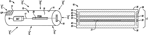
a second conductive layer attached to the first dielectric layer, wherein an electrical current is impressed on the second conductive layer when the PCBA is exposed to an externally generated electric field exterior to the PCBA;
a trans-conductor layer (TCL) attached to the second conductive layer and including a plurality of TCL islands of a nickel-metal composite metamaterial, each of the TCL islands having a distinct shape providing a respective impedance value in response to a variation in an intensity and/or a wavelength of the externally generated electric field;
a second dielectric layer attached to the TCL such that the TCL is positioned between the second dielectric layer and the second conductive layer; and
a pre-pregnated layer, wherein the first dielectric layer is mounted to an inside surface of the first conductive layer, the pre-pregnated layer is mounted to an inside surface of the first dielectric layer, the second conductive layer is mounted to an inside surface of the pre-pregnated layer, the TCL is mounted to an inside surface of the second conductive layer, and the second dielectric layer is mounted to an inside surface of the TCL,
wherein the TCL has a surface roughness configured to change in response to an energy level of the externally generated electric field to thereby change an effective permittivity of the second dielectric layer and thereby direct the impressed electrical current away from the second conductive layer.
|