| CPC H05K 5/03 (2013.01) [G06F 1/1626 (2013.01)] | 14 Claims |

|
1. A rear plate for forming a rear exterior surface of an electronic device, including:
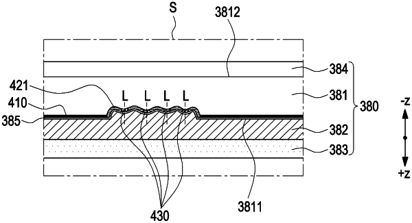
a glass plate including a pattern area, the pattern area including a pattern having a designated shape, in at least a partial area of the glass plate;
a shielding layer disposed at a first side of the glass plate, for shield light directed to an exterior or an interior of the electronic device;
a printed layer disposed between the shielding layer and the glass plate; and
a coating layer disposed at a second side of the glass plate opposite to the first side; and
a transparent member layer disposed between the glass plate and the printed layer, and including a dielectric layer disposed in contact with the glass plate and formed of an acrylic adhesive,
wherein the pattern area of the glass plate includes a plurality of lines spaced apart from each other, wherein the plurality of lines is formed along a direction of virtual lines (L) perpendicular to a surface of the glass plate, and each of the virtual lines (L) of each of the plurality of lines are arranged in a direction parallel to the surface of the glass plate, and
wherein the plurality of lines protrudes toward the transparent member layer and is disposed in contact with the transparent member layer.
|