| CPC H05K 1/09 (2013.01) [C25D 3/38 (2013.01); H05K 2201/0355 (2013.01)] | 6 Claims |
|
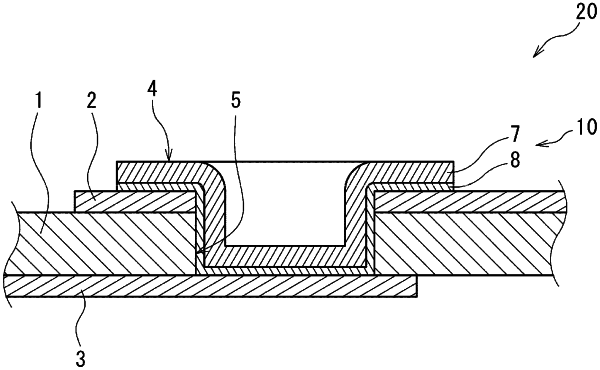
1. A printed circuit board comprising:
an insulating base layer;
a first conductive layer that is stacked on a front surface of the base layer either directly or indirectly and that includes copper foil;
a second conductive layer that is stacked on a back surface of the base layer either directly or indirectly and that includes copper foil; and
a via-hole laminate that is stacked on an inner circumference and a bottom of a connection hole extending through the first conductive layer and the base layer in a thickness direction and that electrically connects the first conductive layer to the second conductive layer,
wherein the via-hole laminate has an electroless copper plating layer that is stacked on the inner circumference and the bottom of the connection hole and an electrolytic copper plating layer stacked on a surface of the electroless copper plating layer,
the copper foil contains copper crystal grains oriented in a (100) plane orientation, and an average crystal grain size of copper of the copper foil is 10 μm or more,
the electroless copper plating layer includes palladium and tin, and
an amount of the palladium stacked per unit area of a surface of the copper foil is 0.18 μg/cm2 or more and 0.40 μg/cm2 or less.
|