| CPC H05K 1/0277 (2013.01) [G02F 1/1676 (2019.01); G06F 3/0445 (2019.05); H05K 3/1275 (2013.01); H05K 3/1283 (2013.01); H05K 3/388 (2013.01); G02F 1/167 (2013.01); G02F 1/16757 (2019.01); G06F 3/0446 (2019.05); G06F 2203/04102 (2013.01); H05K 1/0274 (2013.01); H05K 1/097 (2013.01); H05K 3/282 (2013.01); H05K 2201/037 (2013.01)] | 20 Claims |
|
1. A conductive film comprising a transparent substrate and a conductive part comprising a fine metal wire pattern disposed on one side or both sides of the transparent substrate, wherein
the fine metal wire pattern is constituted by a fine metal wire, and
the conductive film satisfies the following condition (1) or (ii):
(i) the fine metal wire has voids, and when the cross-sectional area of the fine metal wire is defined as SM and the total cross-sectional area of the voids included in the cross-section of the fine metal wire is defined as SVtotal on the cross-section of the fine metal wire perpendicular to the direction of drawing of the fine metal wire, SVtotal/SM is 0.10 or more and 0.40 or less; and
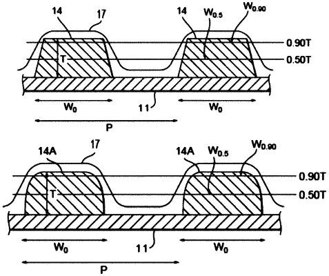
(ii) when the maximum thickness of the fine metal wire on the cross-section of the fine metal wire perpendicular to the direction of drawing of the fine metal wire is defined as T, the width of the fine metal wire at a height of 0.90T from the fine metal wire interface on the transparent substrate side is defined as W0.90 and the width of the fine metal wire on the fine metal wire interface on the transparent substrate side is defined as W0, W0.90/W0 is 0.40 or more and 0.90 or less.
|