| CPC H04N 25/75 (2023.01) [H01L 27/14612 (2013.01); H01L 27/14643 (2013.01); H04N 25/76 (2023.01); H01L 31/107 (2013.01)] | 19 Claims |
|
1. An image sensor, comprising:
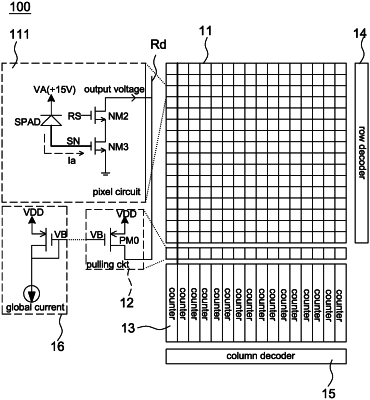
a pixel array comprising a plurality of pixel circuits arranged in a matrix, each of the pixel circuits comprising:
an avalanche diode having an anode and a cathode, the cathode being connected to a positive bias voltage;
a resistive transistor, a drain of the resistive transistor connected to the anode of the avalanche diode, and a gate of the resistive transistor configured to receive a fixed voltage signal;
a first switch transistor, a drain of the first switch transistor connected to a source of the resistive transistor, a gate of the first switch transistor configured to receive an exposure signal, and a source of the first switch transistor connected to a ground voltage;
a pull down transistor, a gate of the pull down transistor connected to the anode of the avalanche diode, and a source of the pull down transistor connected to the ground voltage; and
a second switch transistor, a gate of the second switch transistor configured to receive the exposure signal, a source of the second switch transistor connected to a drain of the pull down transistor, and a drain of the second switch transistor configured to generate an output voltage; and
a plurality of readout lines each being coupled to the drain of the second switch transistor of each pixel circuit of one pixel circuit column to output the output voltage.
|