| CPC H04N 25/13 (2023.01) [H04N 25/589 (2023.01); H04N 25/704 (2023.01)] | 15 Claims |

|
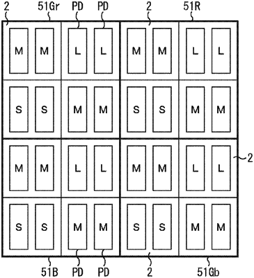
1. A light detecting device comprising:
a first pixel set including:
first through ninth pixels arranged in a first three-by-three matrix in a plan view, each of the first through ninth pixels including two photoelectric conversion parts, and
a first charge holding part coupled to the two photoelectric conversion parts of at least three pixels of the first through ninth pixels in the first pixel set, wherein
a first subset of the first through ninth pixels is arranged to be set at a first exposure time,
a second subset of the first through ninth pixels is arranged to be set at a second exposure time that is shorter than the first exposure time, and
a third subset of the first through ninth pixels is arranged to be set at a third exposure time that is shorter than the second exposure time;
a second pixel set including:
tenth through eighteenth pixels arranged in a second three-by-three matrix in the plan view, each of the tenth through eighteenth pixels including two photoelectric conversion parts, and
a second charge holding part coupled to the two photoelectric conversion parts of at least three pixels of the tenth through eighteenth pixels in the second pixel set;
a third pixel set including:
nineteenth through twenty-seventh pixels arranged in a third three-by-three matrix in the plan view, each of the nineteenth through twenty-seventh pixels including two photoelectric conversion parts, and
a third charge holding part coupled to the two photoelectric conversion parts of at least three pixels of the nineteenth through twenty-seventh pixels in the third pixel set; and
a fourth pixel set including:
twenty-eighth through thirty-sixth pixels arranged in a fourth three-by-three matrix in the plan view, each of the twenty-eighth through thirty-sixth pixels including two photoelectric conversion parts, and
a fourth charge holding part coupled to the two photoelectric conversion parts of at least three pixels of the twenty-eighth through thirty-sixth pixels in the fourth pixel set; wherein
the first, second, third, and fourth pixel sets are arranged in a two-by-two array in the plan view,
the first and fourth pixel sets are configured to produce pixel signals corresponding to light in a first range of wavelengths,
the second pixel set is configured to produce pixel signals corresponding to light in a second range of wavelengths different than the first range of wavelengths, and
the third pixel set is configured to produce pixel signals corresponding to light in a third range of wavelengths different than the first and second range of wavelengths.
|