US 11,876,933 B2
Event image sensor, imaging device, and method of controlling event image sensor
Atsumi Niwa, Kanagawa (JP)
Assigned to Sony Semiconductor Solutions Corporation, Kanagawa (JP)
Filed by Sony Semiconductor Solutions Corporation, Kanagawa (JP)
Filed on Jan. 13, 2023, as Appl. No. 18/096,658.
Application 18/096,658 is a continuation of application No. 16/964,676, granted, now 11,582,408, previously published as PCT/JP2018/046045, filed on Dec. 14, 2018.
Claims priority of application No. 2018-014228 (JP), filed on Jan. 31, 2018.
Prior Publication US 2023/0156356 A1, May 18, 2023
This patent is subject to a terminal disclaimer.
Int. Cl. H04N 25/47 (2023.01); H04N 5/76 (2006.01); H04N 5/77 (2006.01); H04N 25/53 (2023.01); H04N 23/667 (2023.01); H04N 25/50 (2023.01); H04N 25/77 (2023.01); H04N 25/707 (2023.01); H04N 23/71 (2023.01); B60R 11/04 (2006.01)
CPC H04N 25/47 (2023.01) [H04N 5/76 (2013.01); H04N 5/772 (2013.01); H04N 23/667 (2023.01); H04N 23/71 (2023.01); H04N 25/50 (2023.01); H04N 25/53 (2023.01); H04N 25/707 (2023.01); H04N 25/77 (2023.01); B60R 11/04 (2013.01)] 13 Claims
OG exemplary drawing
 
1. A light detecting device, comprising:
a pixel array including a plurality of areas, each of the areas including at least one pixel that detects a change in luminance of incident light occurring outside a dead band as an address event; and
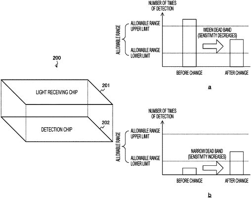
a processor configured to control a width of the dead band according to a number of times the address event is detected for the at least one pixel within a time period.