| CPC H04L 25/03057 (2013.01) [H04L 25/03267 (2013.01)] | 19 Claims |
|
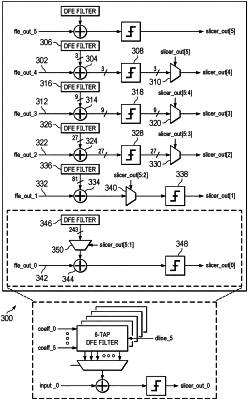
1. A decision feedback equalizer (DFE) comprising:
an N-bit parallel input adapted to be coupled to a communication channel and configured to receive consecutive communication symbols transmitted at a rate of one symbol per cycle during a current clock cycle and each of previous (N−1) clock cycles, wherein N is an integer 5 or greater;
a first DFE path including:
a first path input configured to receive a first one of the communication symbols;
a first adder having a first adder input coupled to the first path input, second adder inputs, and first adder outputs;
first DFE filter circuitry having first DFE filter inputs and having first DFE filter outputs coupled to the second adder inputs and responsive to the first DFE filter inputs, each first DFE filter input has one of three values, and each first DFE filter output corresponds to a member of a set of possible combinations of the first DFE filter inputs;
first slicer circuitry having first slicer inputs coupled to the first adder outputs, and having first slicer outputs; and
a first multiplexer having first multiplexer inputs coupled to the first slicer outputs, a first multiplexer output, and the first multiplexer configured to connect one of the first multiplexer inputs to the first multiplexer output; and
a second DFE path including:
a second path input configured to receive a second communication symbol;
a second adder having a third adder input coupled to the second path input, fourth adder inputs, and second adder outputs;
second DFE filter circuitry having second DFE filter inputs and having second DFE filter outputs coupled to the fourth adder inputs and responsive to the second DFE filter inputs, each second DFE input has one of the three values, and each second DFE filter output corresponds to a member of a set of possible combinations of the second DFE filter inputs;
second slicer circuitry having second slicer inputs coupled to the second adder outputs, and having second slicer outputs; and
a second multiplexer having second multiplexer inputs coupled to the second slicer outputs, a second multiplexer output, and the second multiplexer configured to connect one of the second multiplexer inputs to the second multiplexer output.
|