| CPC H03K 5/134 (2014.07) [H03L 7/0818 (2013.01); H03K 2005/00195 (2013.01)] | 18 Claims |

|
9. A circuit for updating a delay line code, comprising:
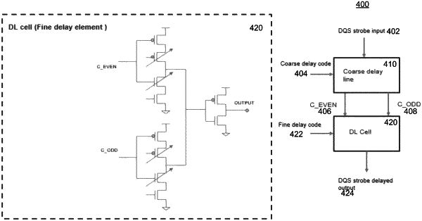
a coarse delay line having a first chain of interleaved logic gates and a second chain of interleaved logic gates, the coarse delay line configured to receive a strobe input and a coarse delay cell code;
a first clock signal generated based upon the first chain of interleaved logic gates;
a second clock signal generated based upon the second chain of interleaved logic gates;
a fine delay cell in electronic communication with the coarse delay cell, the fine delay cell configured to receive the first clock signal, the second clock signal, and a fine delay cell code; and
a strobe delayed output generated based upon, at least in part, the first clock signal, the second clock signal, and the fine delay code;
wherein if the strobe delayed output depends on the second clock signal, a clock on the first clock signal is switched and a number of logic gates is increased to increase a delay on the first chain of interleaved logic gates.
|