| CPC H03B 5/06 (2013.01) [H03B 5/362 (2013.01); H03B 5/366 (2013.01); H03B 2200/0062 (2013.01); H03B 2200/0082 (2013.01)] | 20 Claims |
|
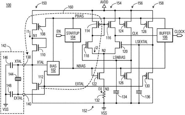
1. A crystal oscillator circuit comprising:
a gain stage circuit coupled between a first voltage supply terminal and a second voltage supply terminal, the gain stage circuit having a first gain stage input coupled at a first oscillator terminal and configured to receive a first oscillator signal of a crystal;
a first bias circuit having an input coupled at the first gain stage input and an output, the bias circuit configured to generate a first bias voltage based on the first oscillator signal;
a reference circuit having an input coupled at the output of the first bias circuit, the reference circuit configured to generate a reference current based on the first bias voltage; and
a comparator circuit coupled to the reference circuit at a first node, the comparator circuit configured to generate a clock signal at a comparator output based on the first oscillator signal and the first bias voltage, the comparator circuit including a second bias circuit configured to generate a second bias voltage, the gain stage circuit having a second gain stage input coupled to receive the second bias voltage.
|