| CPC H02P 27/08 (2013.01) [H02P 21/22 (2016.02)] | 4 Claims |

|
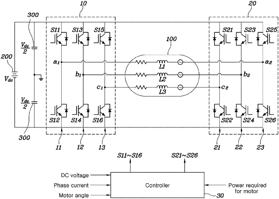
1. A motor driving apparatus configured to drive a motor including a plurality of windings respectively corresponding to a plurality of phases, the apparatus comprising:
a first inverter including a plurality of first switching elements and connected to a first end of each of the windings;
a second inverter including a plurality of second switching elements and connected to a second end of each of the windings; and
a controller configured to obtain a voltage command vector, which is a vector corresponding to a voltage command of the motor, by combining switching vectors which cause difference between a common mode voltage of the first inverter and a common mode voltage of the second inverter to be zero and configured to control the plurality of first switching elements and the plurality of second switching elements in a pulse width modulation method based on the obtained voltage command vector,
wherein the switching vectors include a total of 64 switching vectors by combining eight voltage vectors which are combined by the first inverter and eight voltage vectors which are combined by the second inverter, and
wherein the switching vectors which cause the common mode voltage difference to be zero of the 64 switching vectors include:
a switching vector in which a switching state of the first inverter is [1001 and a switching state of the second inverter is [0101;
a switching vector in which the switching state of the first inverter is [1001 and the switching state of the second inverter is [0011;
a switching vector in which the switching state of the first inverter is [1101 and the switching state of the second inverter is [0111;
a switching vector in which the switching state of the first inverter is [1101 and the switching state of the second inverter is [1011;
a switching vector in which the switching state of the first inverter is [0101 and the switching state of the second inverter is [0011;
a switching vector in which the switching state of the first inverter is [0101 and the switching state of the second inverter is [1001;
a switching vector in which the switching state of the first inverter is [0111 and the switching state of the second inverter is [101];
a switching vector in which the switching state of the first inverter is [011] and the switching state of the second inverter is [110];
a switching vector in which the switching state of the first inverter is [001] and the switching state of the second inverter is [100];
a switching vector in which the switching state of the first inverter is [001] and the switching state of the second inverter is [010];
a switching vector in which the switching state of the first inverter is [101] and the switching state of the second inverter is [110]; and
a switching vector in which the switching state of the first inverter is [101] and the switching state of the second inverter is [011],
wherein first, second, third digits of numbers indicating the switching states indicate the switching states of the switching elements in phases a, b, and c, respectively, in each of the first inverter and the second inverter, and a number “1” indicates that an upper switching element of an associated phase is turned on and a lower switching element thereof is turned off, and a number “0” indicates that the upper switching element of the associated phase is turned off and the lower switching element thereof is turned on.
|