| CPC H02M 3/158 (2013.01) [H02M 1/0016 (2021.05); H02M 1/15 (2013.01)] | 19 Claims |

|
1. A DC-DC converter, comprising:
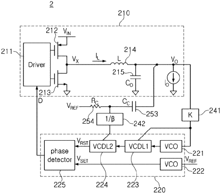
a switching buck regulator including a first power switch connected to a first power node for outputting a first power voltage, a second power switch connected to a second power node for outputting a second power voltage lower than the first power voltage, a driver configured to drive the first power switch and the second power switch, an output filtering inductor connected to a node between the first power switch and the second power switch, and an output filtering capacitor connected to the output filtering inductor;
a controller configured to compensate for an output signal of the switching buck regulator in a time domain using a reference voltage; and
a circuit connected between the switching buck regulator and the controller, the circuit including a first buffer, an RC filter, a second buffer, and an adder sequentially on a path,
wherein an input terminal of the first buffer is connected to an output terminal of the switching buck regulator and the adder, and an output terminal of the first buffer is connected to the RC filter, and
an input terminal of the second buffer is connected to the RC filter and the controller, and an output terminal of the second buffer is connected to the adder.
|