US 11,876,391 B2
Circuits and methods for wearable device charging and wired control
Yu Jiang Tham, Los Angeles, CA (US); Nicholas Larson, Playa Vista, CA (US); Peter Brook, Marina del Rey, CA (US); Russell Douglas Patton, Marina Del Rey, CA (US); Miran Alhaideri, Los Angeles, CA (US); and Zhihao Hong, Marina Del Rey, CA (US)
Assigned to SNAP INC, Santa Monica, CA (US)
Filed by Snap Inc., Santa Monica, CA (US)
Filed on Feb. 5, 2021, as Appl. No. 17/168,797.
Application 17/168,797 is a continuation of application No. 16/829,567, filed on Mar. 25, 2020, granted, now 10,938,151.
Application 16/829,567 is a continuation of application No. 16/250,984, filed on Jan. 17, 2019, granted, now 10,637,183.
Application 16/250,984 is a continuation of application No. 15/782,575, filed on Oct. 12, 2017, granted, now 10,218,114.
Claims priority of provisional application 62/407,374, filed on Oct. 12, 2016.
Prior Publication US 2021/0194178 A1, Jun. 24, 2021
This patent is subject to a terminal disclaimer.
Int. Cl. H02J 7/00 (2006.01); H02J 7/04 (2006.01); H04B 3/56 (2006.01); G02C 5/14 (2006.01); G02C 11/00 (2006.01); H01L 27/02 (2006.01); H01R 13/62 (2006.01); H03K 19/0185 (2006.01); H02J 7/34 (2006.01); H04B 3/54 (2006.01); G02C 1/00 (2006.01)
CPC H02J 7/0034 (2013.01) [G02C 5/146 (2013.01); G02C 11/10 (2013.01); H01L 27/0266 (2013.01); H01R 13/6205 (2013.01); H02J 7/0045 (2013.01); H02J 7/0068 (2013.01); H02J 7/04 (2013.01); H02J 7/345 (2013.01); H03K 19/018557 (2013.01); H04B 3/56 (2013.01); G02C 1/00 (2013.01); H02J 7/00 (2013.01); H02J 7/00034 (2020.01); H02J 7/00302 (2020.01); H02J 7/00306 (2020.01); H04B 3/548 (2013.01); H04B 2203/547 (2013.01); H04B 2203/5454 (2013.01)] 20 Claims
OG exemplary drawing
 
1. A wearable device comprising:
a charge interface comprising a first charge pad and a second charge pad; and
circuitry coupled to the first charge pad and the second charge pad, wherein the circuitry is configured to:
perform a charging process where the wearable device receives an electrical charge from a device to charge a battery via the first charge pad and the second charge pad;
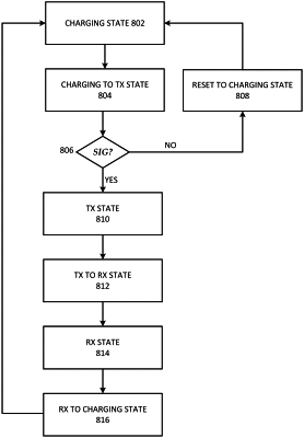
cause a transition signal to be sent via the first charge pad or the second charge pad to the device; and
transmit data via the first charge pad or the second charge pad to the device.