| CPC H01L 33/502 (2013.01) [H01L 25/0753 (2013.01); H01L 27/156 (2013.01); H01L 33/483 (2013.01); H01L 33/54 (2013.01); H01L 33/56 (2013.01); H01L 33/58 (2013.01); H01L 33/60 (2013.01); H01L 33/62 (2013.01); H01L 33/641 (2013.01); H01L 25/167 (2013.01); H01L 2224/16 (2013.01)] | 18 Claims |
|
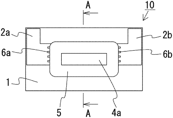
1. A light emitting apparatus comprising:
an electrically insulating base member having, in a top plan view, a first edge, a second edge opposite the first edge, a third edge, and a fourth edge opposite the third edge, wherein the first and second edges of the base member extend in a first direction, and the third and fourth edges of the base member extend in a second direction;
first and second electrically conductive pattern portions formed on an upper surface of the base member;
at least one light emitting device that is electrically connected to the first and second electrically conductive pattern portions;
a transparent member disposed on the at least one light emitting device; and
a resin portion that surrounds the transparent member in the top plan view, and that partially covers the first and second electrically conductive pattern portions, wherein the resin portion has, in the top plan view, a first edge on a side corresponding the first edge of the base member, a second edge opposite the first edge, a third edge on a side corresponding to the third edge of the base member, and a fourth edge opposite the third edge, wherein the first and second edges of the resin portion extend in the first direction, and the third and fourth edges of the resin portion extend in the second direction;
wherein, in the top plan view:
a part of the first electrically conductive pattern portion is exposed from the resin portion, extends along the third edge of the base member, and is located between (i) the first edge of the base member, and (ii) a line along which the first edge of the resin portion extends, and
a part of the second electrically conductive pattern portion is exposed from the resin portion, extends along the fourth edge of the base member, and is located between (i) the first edge of the base member, and (ii) the line along which the first edge of the resin portion extends.
|