| CPC H01L 33/46 (2013.01) [G02F 1/133603 (2013.01); G02F 1/133605 (2013.01); G02F 1/133607 (2021.01); G02F 1/133614 (2021.01); H01L 25/0753 (2013.01); H01L 33/42 (2013.01); H01L 33/502 (2013.01); H01L 33/505 (2013.01); H01L 33/54 (2013.01); H01L 33/56 (2013.01); H01L 33/58 (2013.01); H01L 33/60 (2013.01); H01L 33/62 (2013.01); H01L 2933/005 (2013.01); H01L 2933/0025 (2013.01); H01L 2933/0041 (2013.01); H01L 2933/0091 (2013.01)] | 20 Claims |

|
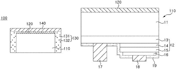
1. A display apparatus, comprising:
a display panel; and
a backlight configured to provide light toward the display panel, the backlight comprising:
a circuit board;
an optical layer disposed on the circuit board;
at least one light emitter disposed between the circuit board and the optical layer, the light emitter comprising:
a light emitting structure disposed on the circuit board and having a first conductivity type semiconductor layer, a second conductivity type semiconductor layer, and an active layer disposed between the first conductivity type semiconductor layer and the second conductivity type semiconductor layer;
a first electrode pad electrically connected to the first conductivity type semiconductor layer of the light emitting structure; and
a second electrode pad electrically connected to the second conductivity type semiconductor layer of the light emitting structure;
a reflector disposed on the light emitting structure;
a light transmitting layer disposed on the circuit board and contacting the light emitter; and
a dam disposed on the circuit board and surrounding the light emitter, wherein the dam has a portion having a curved shape.
|