| CPC H01L 33/32 (2013.01) [H01L 33/04 (2013.01)] | 20 Claims |
|
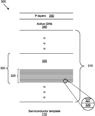
1. A light-emitting diode (LED) structure formed on a substrate, the LED structure comprising:
a strain management region supported on the substrate; and
an active region configured to provide a light emission associated with the LED structure,
wherein the strain management region includes a plurality of sets of layers,
each set of layers from the plurality of sets of layers including:
a first layer including a superlattice having a plurality of repeated first sublayers and second sublayers, and
a second layer including a bulk layer.
|