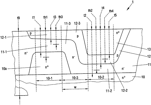
| CPC H01L 31/1105 (2013.01) [H01L 31/18 (2013.01)] | 16 Claims |

|
1. A method of forming a photosensitive semiconductor component, the method comprising:
(i) providing a semiconductor substrate of a first conductivity type as a collector layer;
(ii) forming a less doped layer of the first conductivity type above the semiconductor substrate;
(iii) forming a semiconductor base layer of a second conductivity type therein or thereabove;
(iv) forming an emitter layer of the first conductivity type therein or thereabove, such that a part of the base layer is not covered by the emitter layer,
wherein at least one of the less doped layer or the semiconductor base layer is formed with regions of different thicknesses including a region of greatest thickness and a region of smaller thickness that has a thickness that is smaller than the thickness of the region of greatest thickness, and thereafter the emitter layer is formed in the region having the greatest thickness of the at least one of the less doped layer or the semiconductor base layer, wherein the emitter layer is formed with a thickness which is greater than the smaller thickness of the at least one of the less doped layer or the semiconductor base layer.
|